Amplifier Design
December 15, 2023
2nd Place Winner in the 2023 Analog Devices IC Design Contest
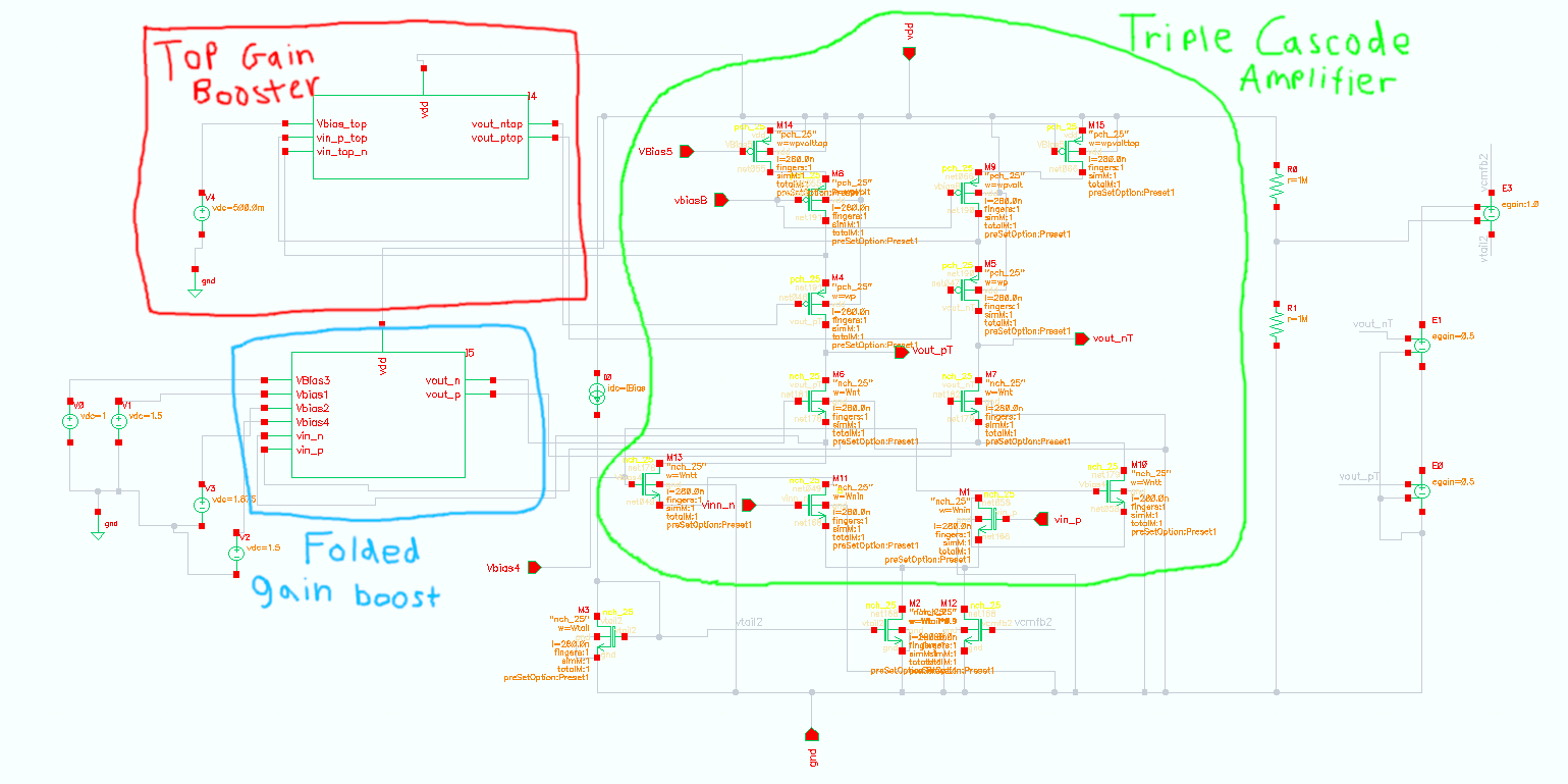
For the 2023 Analog Devices IC Design Contest, my partner (William Schilp) and I designed a triple cascode amplifier that included a gain boosting circuit on the PMOS side and folded gain booster on the NMOS side.
Much was learned throughout this project. I’d say the most important takeaway is that analog circuit design is a very sensitive process. Even the smallest changes in design parameters can have an enormous impact on the functionality of the circuit.
Our final circuit (designed on a typical 65nm process) achieved a gain of 86dB, ~75 degrees phase margin, 562 MHz Unity Gain Frequency, and an output swing of 935 mV, while consuming 35 mW of power.
Due to constraints imposed by the design contest, we were unable to implement several improvements that would have greatly enhanced the performance of our amplifier. Mainly, our output swing was severely limited by the PMOS side gain booster. This circuit was implemented as a common source amplifier. Had it been implemented as a folded cascode amplifier with an NMOS input structure, we believe we would have both increased our circuit’s stability and output swing.
We also think that with a bit more optimization of our base triple cascode amplifier, we could have greatly reduced the power consumption of our circuit.
All in all, this project was a great learning experience and a lot of fun. We are very proud of our final design and the performance we were able to achieve.